Computer Architecture Basics
Circuitry
Using just two transistors and a resistor, we can create a circuit called a NAND gate. If either of its inputs are low, the connection to ground is broken, and the voltage at its output stays high. It’s only when both of its inputs are high, it shorts to ground and the voltage at its output is low. It doesn’t seem like much.
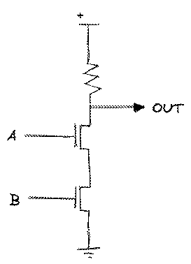
| A | B | OUT |
|---|---|---|
0 |
0 |
1 |
0 |
1 |
1 |
1 |
0 |
1 |
1 |
1 |
0 |
However, starting from that single NAND gate, we can create other atomic logic gates AND, OR, NOT, and XOR (exclusive OR). From there, we can build more complicated operations like multiplexers (MUX) and demultiplexers (DMUX). We can also combine these in various ways to create components which operate on many bits at once.
For a computer to be useful, it would be nice if it were possible to manipulate more data than just a single 1 or 0. Using binary, it’s possible to deal with numbers, and if we allow numbers represent letters and other glyphs, we can deal with text. We can combine the elementary gates above in various ways to expand these operators to affect these larger values.
Further Topics
- Two’s complement (negation, subtraction)
The ALU
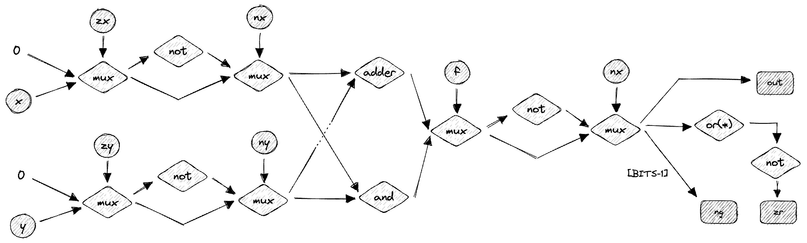
The simplest arithmetic logic unit (ALU) consists of two data and one function input, and combines are few circuits to compose any logical or mathematical operations necessary to be useful within a computer’s processor. The Hack ALU described in the Nand2Tetris course attempts to accomplish this in a direct, elegant way. It’s function input uses just 6 bits as directives that shape resulting operation. These basic directives include:
| Description | |
|---|---|
zx |
Zero the x input, otherwise leave the same |
nx |
Negate the x input |
zy |
Zero the y input |
ny |
Negate the y input |
f |
x+y if f else x&y |
no |
Negate the output of f |
With the six inputs shown above, it’s possible to perform logical and mathematical operations on two inputs x and y. It is also possible to force x or y to all 0 or 1 bits, and thanks to two’s complement, it’s trivial to implement incrementers and decrementer using NOTs and adders. In effect, it turns out operate like so:
MAX_BITS     = 0b11111111;
plusOne      = n => ~(~n + MAX_BITS) & MAX_BITS;
minusOne     = n => (n + MAX_BITS) & MAX_BITS;
makeNegative = n => ~(n + MAX_BITS) & MAX_BITS;
The ALU also has two additional outputs, that can be used later as control flags to perform comparisons.
| Description | |
|---|---|
zr |
Output is 0 |
ng |
Output is negative |
Altogether, the ALU looks something like this:
Memory
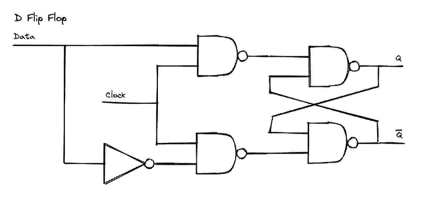
The ALU deals exclusively with combinatorial logic, however to really be useful, a computer also needs to perform more complex multi-step operations. To do this, we must implement sequential logic. The essence of sequential logic is treating the output of each step as the input for the next: $$state_t = fn(state_{t-1})$$ A D Latch allows its output to be changed while its enable input is high. When the enable input goes low, it stays latched to its current state. A D Flip Flop is a D Latch whose enable input is the output of an oscillating (i.e. clocked) edge-detector circuit.
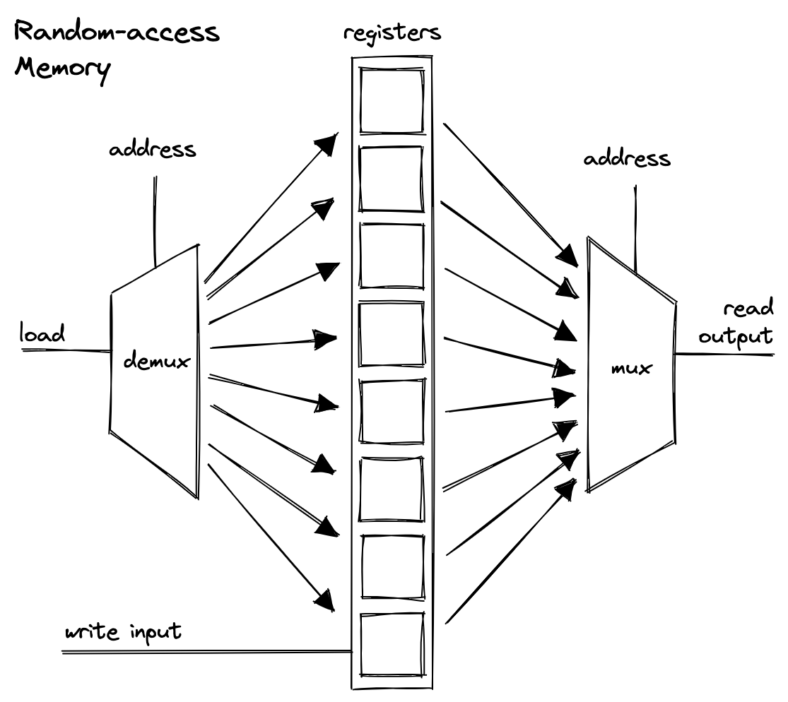
Using the D Flip Flop, we can create a 1-bit Register by multiplexing the input and a feedback loop of the output using a load bit as the selector.
💡 Note: It is not as simple as ANDing the clock and load bits due to timing issued caused by the delay of the AND gate.
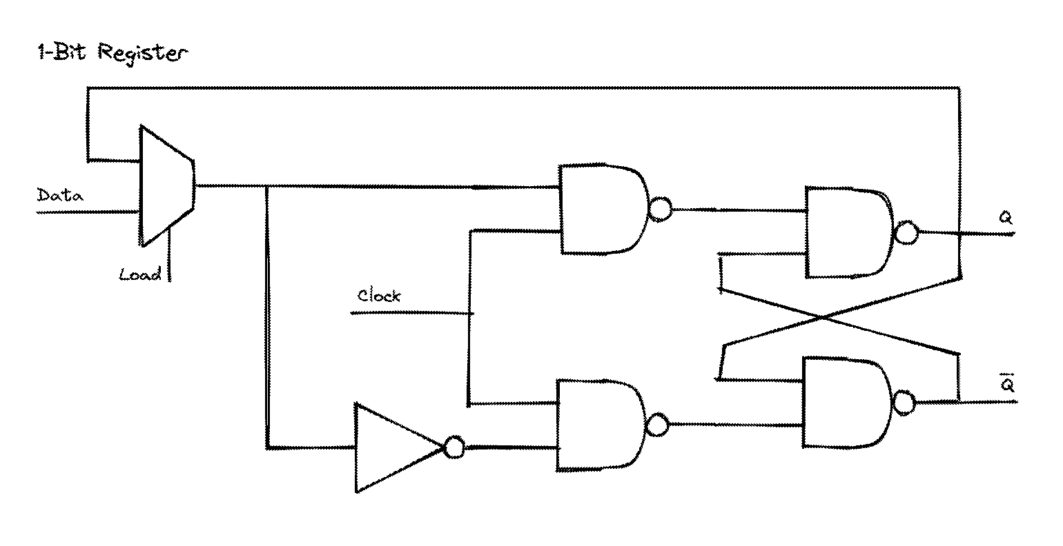
Multi-bit Registers are simply collections of 1-bit registers in parallel, tied to the same load bit. The number of bits in the register is known as its word size. When we talk about a 32- or 64-bit computer, this refers to the word size.
By using multiplexers, it’s possible to organize physical memory into sequences (or multi-dimensional grids but the implementation doesn’t really matter for our purposes) of individually addressable registers. This is what we typically refer to as random-access memory or RAM. It is volatile, meaning it is not persisted between power cycles.
The Program Counter
A counter is a clocked circuit that increments the value that is stored in a register. The program counter (PC) is a specific circuit used to iterate over computer instructions in memory. It can optionally be reset to 0, or accept an input, which allows for arbitrarily jumping around within memory to support loops, conditionals, and subroutines.
The CPU
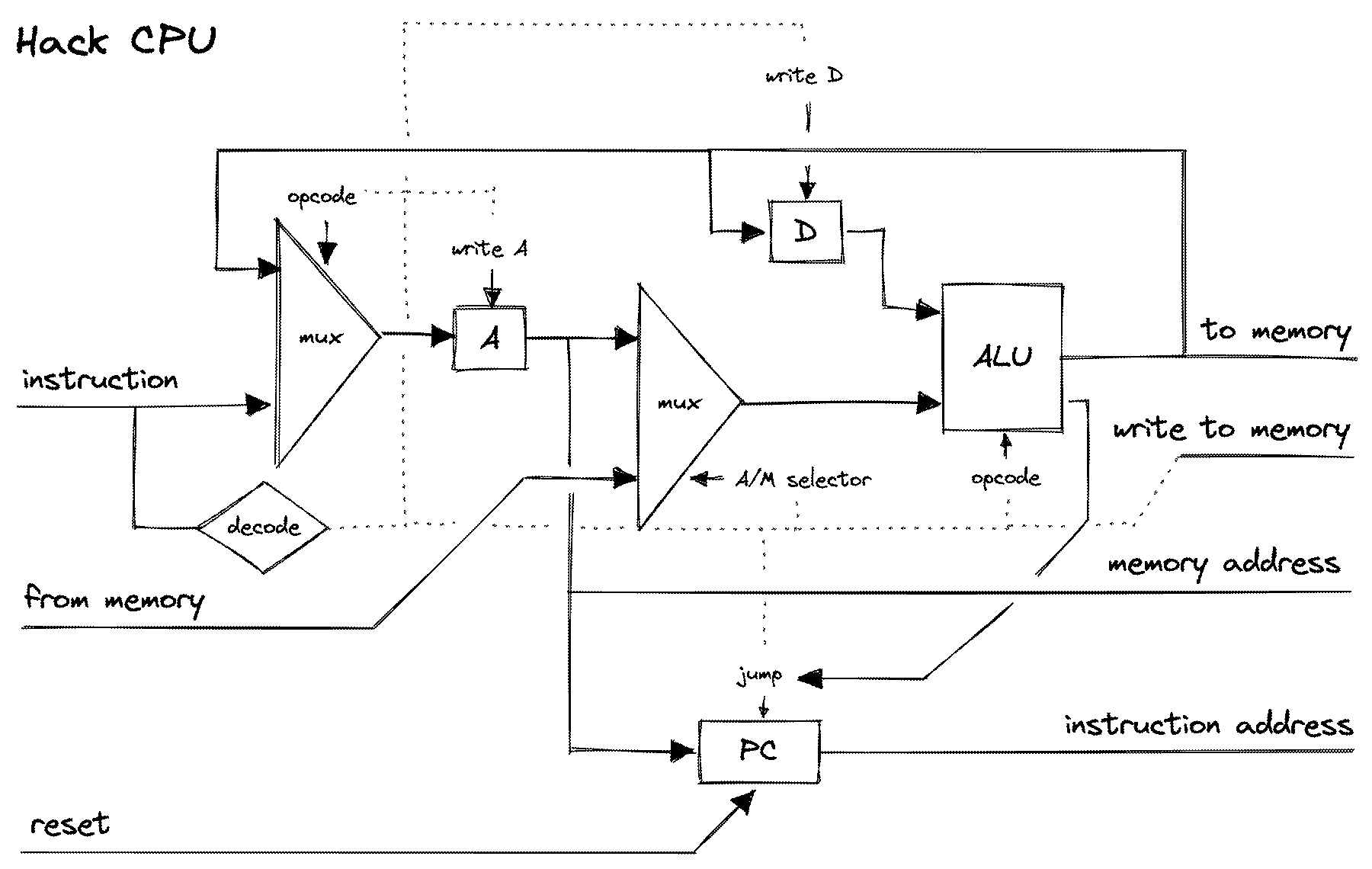
In order to move from more simplistic calculators to a general purpose computational device, a leap was made. Rather than preprogram the instructions within the circuitry or on a plugboard, Alan Turing theorized a universal Turing machine which stored the instructions alongside the rest of the data. As we’ll see, this allows for computation that recurses, forks, jumps, and modifies itself — performing operations that would normally be impossible by a fixed program.
John von Neumann expanded on this for the EDVAC, designing what would eventually be called the von Neumann architecture, combining an ALU, memory (registers and/or RAM), and a program counter along with control circuitry to identify and perform instructions encoded in memory, and busses for these communications to take place.
At its core, CPU instructions are incredibly simple, and are essentially relegated into actions of moving data, performing simple mathematical operations and comparisons, and jumping to other places in memory where instructions can be read. It performs these actions one by one in a loop from the instant you turn a computer on to when it’s powered down. We call this loop the fetch-execute cycle or the fetch-decode-execute cycle.
- Read instruction from the memory address contained by the program counter
- Store instruction in instruction register
- (Optional) Decode instruction into one or more machine operations
- Execute instruction against source and destination
- Send data from appropriate sources into the ALU
- Accept output from the ALU in the requested destination
- Repeat
These instructions are referred to as the computer’s instruction set. It usually a binary representation consisting of an arithmetic, logical, or flow control operation and the operands, whether they be a certain CPU register, a memory location, or a static value.
An imaginary example would be that a CPU designer designated a 0x3d byte to mean add the data at register X to the accumulator register. Software developers, or in most of our cases a high-level language compiler would decide an operation requires this addition to occur and would know from the CPU manufacturer’s documentation, that the next instruction in memory should be 0x3d. These instruction sets are different for different processors, which is why you can’t just take a binary executable from a Mac and copy it over to a Raspberry Pi.
Registers and Caches
Every piece of data a computer handles is stored somewhere, whether that’s a CPU register, the CPU cache, main memory, disk storage, even the internet. While it may not always be the case, usually the closer storage is to the ALU, the faster that its data can be accessed. Conversely, the further storage is from the CPU, the more of it there is.
Average Storage
| Storage | Approx. Max Capacity | Access Speed |
|---|---|---|
| Registers | 576 B | 1 cycle |
| L1 Cache | 64 KB | 6 cycles |
| L2 Cache | 20 MB | 20 cycles |
| DDR/Main Memory | 384 GB | 120 cycles |
| Disk | ??? TB | 1,000+ cycles |
| Network | ∞ | > 10ms |
Registers are very fast memory for the CPU and instruction sets are designed to perform actions directly on them. The L* caches are positioned on the CPU die as well, just a bit further off. For processors with multiple cores, each core usually has its own L1 cache, and typically share the other higher level caches between the cores. Memory and disk drives are connected to the system bus, which due to distance and the shared nature of the system bus, make them slower to access. Prior to SSD storage, spinning disk drives were much slower due to the drive having to spin platters to the correct position before reading.
Question: How exactly does the system bus work?
CPUs are designed in ways to make handling instructions faster with caching and pipelining. Without these the CPU would fetch each instruction and its parameters from main memory.
Addressing Modes
The ISA commonly includes multiple instructions for the same operations, but each will target different combinations of registers, memory, and immediate values. Below are examples of addressing modes used in x86 assembly language and its underlying machine code.
| Mode | Example | Description |
|---|---|---|
| Register | add %eax, %ebx |
Add value in register eax to register ebx |
| Direct | add 0xffff, %eax |
Add value at memory address 0xffff to register eax |
| Indirect | add (%eax), %ebx |
Add value at memory address in eax to ebx |
| Immediate | add $4, %eax |
Add 4 to register eax |
The Assembler
The assembler is a piece of software that converts code in an (arguably) human-readable assembly language into binary machine code data and instructions usable by the CPU hardware. Assembly languages establish symbolic meaning to machine language by supporting mnemonics for operations, registers, and variables.
Memory-mapped IO
Many computers map input/output devices to allocated regions of the memory. Usually these things are abstracted to high-level libraries, but at their lowest level, display devices are given dedicated memory space in RAM (they may or may not have their own memory on-board as well) to hold the image, and are refreshed on clock cycles.
Input can be mapped in a similar manner, using a region of memory to contain keypresses, mouse positions, etc.
In progress…
Virtual Machines and Stack Machines
Machine code and the assembly language abstraction above it are specific to a given chipset, meaning that applications must be compiled to each target device’s machine language. Rather than do this for every program, many programmers have turned to virtual machines, essentially a single program that emulates a computer with a generic instruction set.
A stack machine is a common implementation that relies on a stack data structure to hold data instead of registers. Values are pushed to the stack, and operations can pop these values off, use them, and push results back onto the stack. For example:
push constant 2 // stack: 2
push constant 3 // stack: 2, 3
add             // stack: 5
pop 0xffff      // stack: <empty>
                // memory location 0xffff set to 5
Java’s JVM and Python both compile to an intermediary virtual machine bytecode run by a stack machine.
Also see register machines, symbol tables.
Functions
Functions hold their own working stack and memory segments. They are created when the function is called and recycled when the function returns. When called, typically space is allocated on the stack for the call arguments and any local variables and/or memory segment addresses necessary for the function alongside the return address. This is called the stack frame. Below this point, instructions can manipulate the stack, call other functions, etc… Once this is done, the return statement sets the value on the return address and restores the stack pointer back to the caller’s context.
Memory
Assembly language can make it trivial to access any part of the computers RAM. With multiple pieces of software running on a single machine, it’s a disasterous idea to allow any program to access another’s memory (think about all of the stolen passwords, bank account information, etc…).
The operating system provides methods of protection over the physical memory space, and high-level languages structure data types in ways that compile down to simple offsets, and use system calls to abstract away the hassle of manual memory management.
Note: Instantiating objects in high-level languages typically return pointers to address space that is structured for a given complex data type. Its fields are held within this space in predictable offsets.
See Memory for more thorough notes.
Programming Languages
- Tokenizers
- Grammar
- Terminal vs. non-terminal rules
- Context-free grammars
- Determines if the tokens comprise a meaningful structure
- LL/LR
- LL(k): at most k tokens ahead of parser
- Parsers
- Parse trees
- Abstract syntax trees
Operating Systems
Operating systems lie in between user applications and the hardware, performing scheduling, providing access to memory and files, and enforcing security rules like enabling only certain users to access files or making certain files read-only.
Operating systems aren’t exclusively for what we would commonly deem computers but are also made for phones, routers, etc. and are tailored to all of the various architectures, not just Intel and ARM.
The kernel is the core component of the operating system, responsible for managing system resources and assists applications with performing work (memory management, process scheduling). In addition to the kernel, OSes are commonly shipped with a lot of extra user-space software as well.
The operating system is also in charge of allocating CPU time to all of the various applications and running processes.
Scheduler
Operating systems schedulers vary, but often rely on one of a few designs:
A Multi-layer feedback queue (MLFQ) is one strategy for task queuing that assign tasks to specific priority levels. Tasks start at the highest level (this level may be different for kernel and user processes). The scheduler tracks how long the CPU was occupied for a given time slice. For CPU-bound processes, the priority is lowered, while processes that yield for IO stay at a higher priority. This keeps interactivity a top concern for the system. Periodically, all processes will return to their highest priority so CPU-bound processes are not starved by IO.
Time slices are also referred to as quantums, and are measured in periods of time called jiffies.
See also target latency and minimum granularity. Most kernels can also be preempted so they don’t hog the CPU.
Proportional share scheduling attempts to prioritize fairness when allocating resources to processes. Common fail scheduling algorithms include ticketing, stride scheduling, and the Linux Completely Fair Scheduler (CFS), Brain Fuck Scheduler (BFS), and O(1) scheduler.
The Linux CFS attempts to run all scheduled processes within a specified sched_latency value. It utilizes dynamic time slices and priorities (see nice) to calculate a weighted virtual runtime score vruntime for how much CPU time a process has. The processes are stored in a red-black tree so that the processes with the lowest vruntime receive the next execution.
Standard Libraries
- Mathematical operations
- Abstract data types
- I/O
- Graphics and UI
- Command line, windowing system
- Memory management
- Block storage and file systems
- Device drivers
- Multitasking
- Networking
- Security
- Multi-threading, multi-processing
Bootstrapping
Bootstrapping is the process of loading software into memory immediately proceeding startup or reset. This is done with a contract between the computer’s hardware and software.
See BIOS.
Government Analogy
A common analogy for illustrating how the operating system’s kernel prioritizes work is the government. The government is allotted a certain amount of resources in the form of taxes. These resources are used on the citizenry (user-space) by spending money on emergency services, roads, and schools. However, the government also needs to spend some of that money on its internal operating costs like constructing government buildings and paying salaries.
Like a well-functioning government, ideally the operating system should be able to expend some of its resources on itself without noticably impacting the user. Algorithms used by the OS need to be incredibly fast and lightweight.
System Calls
Many systems make a sharp deliniation between user-level procedures and the OS by virtualizing resources and allowing user programs access through system calls. The trigger hardware traps that transfer control from the user mode to the OS to run code at a higher privilege level in kernel mode.
Note that the low-level implementation mechanisms determine how a computer performs context switches, while its high-level policies determine which process gets handled and when.
fork()spawns a copy of the current process into its own address space starting immediately afterforkwas calledwait()blocks until the child process ends, which is useful for coordinating new independent processes (also seewaitpid())exec()runs a different program in-place, meaning that the OS overwrites the current code and reinitializes the process state (see alsoexecl(),execlp(),execle(),execv(),execvp(), andexecvpe())pipe()kill()/signal()
You can build a shell using fork(), exec(), and wait().
Linux:
ps, top, kill, fg
What is a process?
A process is an abstraction of the state of a currently running program, bundling memory address space, register values, program counter, stack/frame pointers, open file handles, etc…
When a program is run, the operating system loads the instructions (either eagerly or lazily) into memory, additional memory is allocated for the runtime stack and the heap.
- On UNIX, three open file descriptors for stdio, stdout, and stderr.
- Entrypoint main().
- Running, blocked, ready states.
- Running -> ready: descheduled
- Ready -> running: scheduled
- Ready -> blocked: IO initiated
- Blocked -> ready: IO done